1) Active Component Design
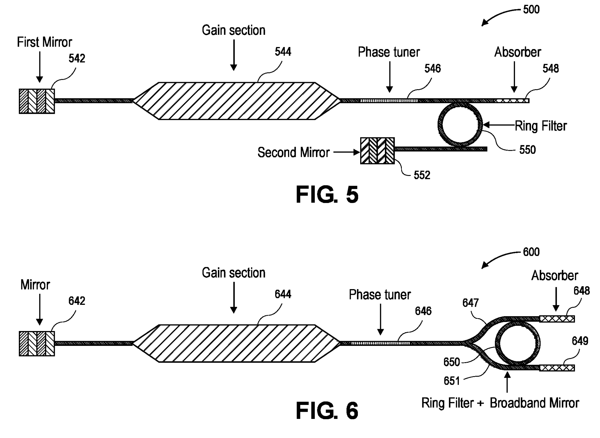
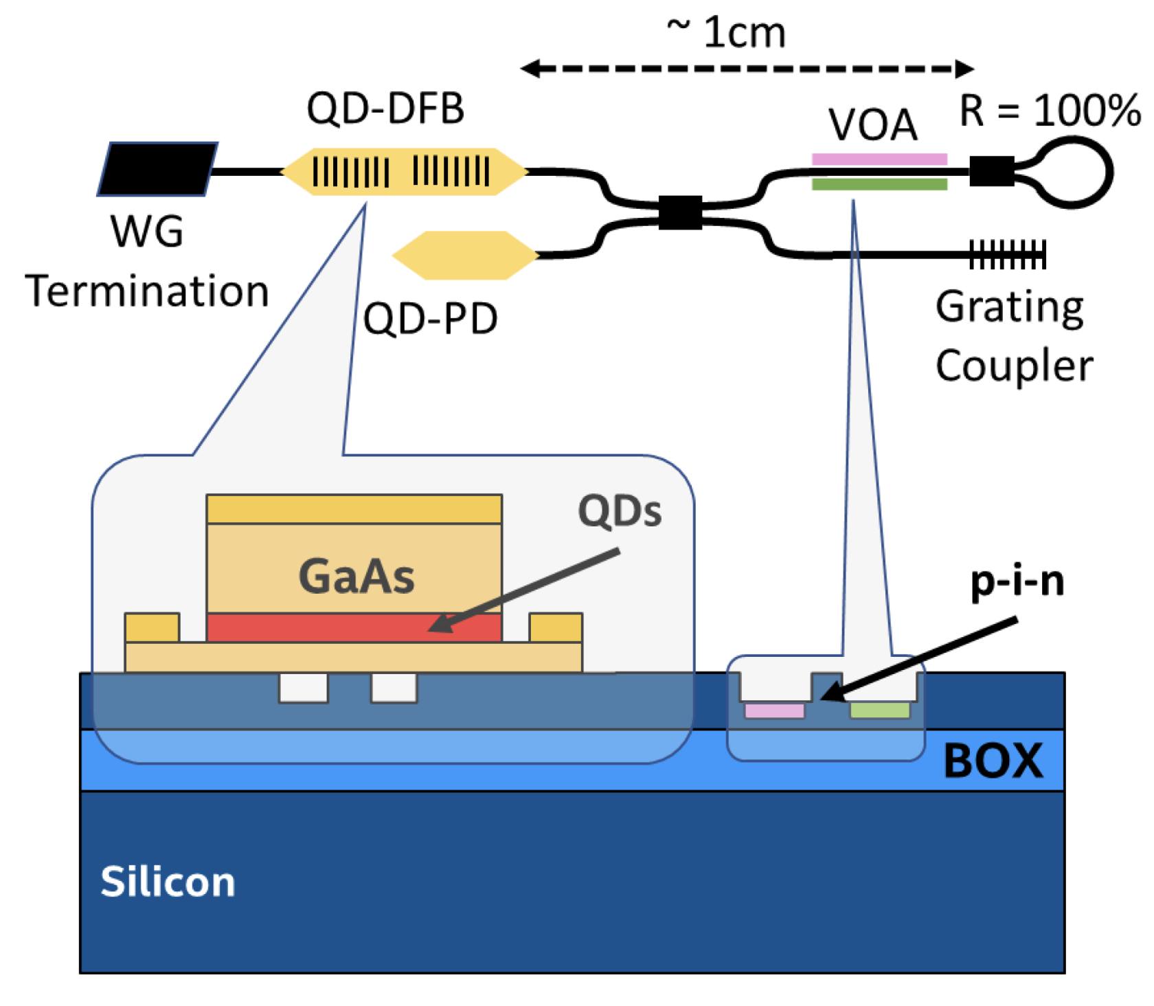
We can design the discrete/integrated light source’s epitaxial structure as well as the photonics integrated circuit needed to test and characterize the device’s performance. We can also design new laser architectures which take advantage of an integrated photonics platform, such as the patented ring-resonator and DBR-coupled multi-wavelength laser.
Each photonics integrated circuit (PIC) requires light sources (lasers, superluminescent diodes, optical amplifiers) and/or optical modulators which are optimized for the specific application and PIC architecture. The design of these components involves collaboration between the component and system designers.
Once the customer communicates the application and device requirements, we can perform a literature survey, device modelling/ simulation, summarize the various device design options to the customer, design the test structures needed to characterize the components’ performance, and guide the customer’s layout team in ensuring that all the component designs and test structures have been correctly laid out.
Mehta et.al, physica status solidi (a) 217, 2000154 (2020)
Mehta et.al, U.S. Patent No. 12,088,060, Sept. 2024.
2) Test Structure Design
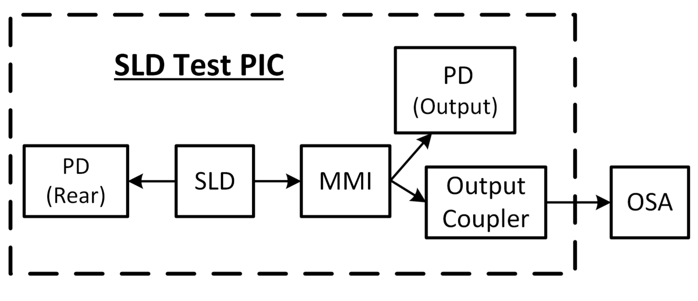
Integrated photonics allows a lot of component-level testing to be done on-chip through the layout of test structures, which simplifies testing compared to discrete optical test setups. Thus, thoughtful design of test structures is a critical part of component design, without which characterizing the component’s performance becomes far more challenging.
Test structures can also be designed for process monitoring by fabs and foundries.
Designing integrated photonics components and test structures requires collaboration between several teams of people with complementary skillsets. It involves component designers, system architects (PIC designers), layout engineers, epitaxy engineers, process engineers, and test engineers. I have experience in end-to-end component development on several projects as the lead light source designer from my tenure at Intel Corporation and Georgia Tech.
Mehta et. al, IEEE Photonics Technology Letters 35 (7), 365-368 (2023)
D. Huang et. al, J. Lightwave Technol 43 (4), 1855-1860 (2025)
3) Photonics Test Development & Performance Analysis
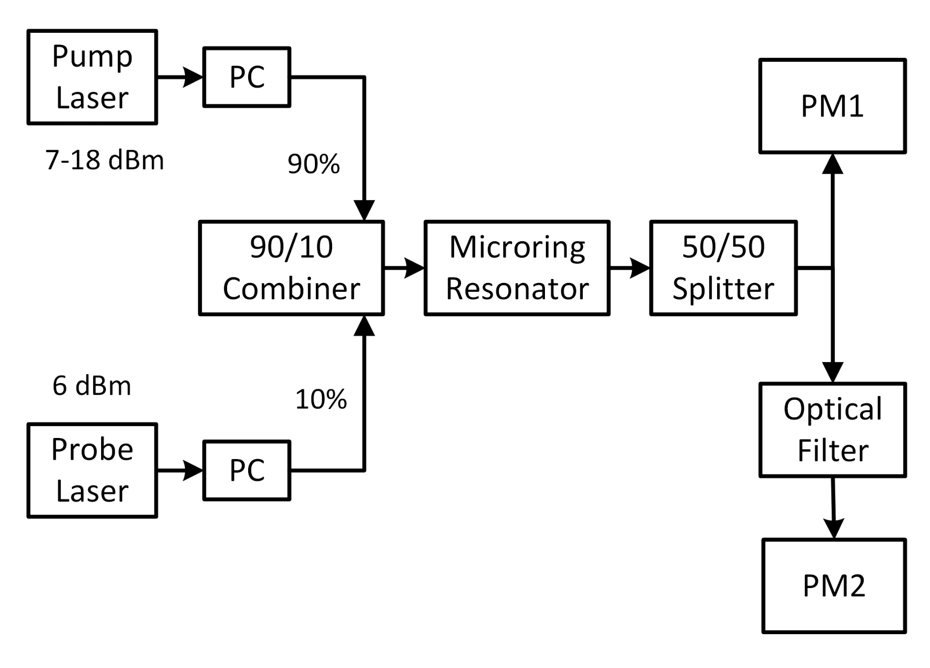
Once the customer defines which component parameters they are interested in measuring, we can work with their designers and test engineers to define a test plan and methodologies to extract the relevant parameters from the measured data.
This service involves designing the test setup, defining the test conditions, and developing a data analysis methodology to extract the relevant device parameters from the measured data. If the customer’s project requires a new test to be developed, we will work with the customer’s test and design teams to bring up the test and data analysis methodology, and to subsequently validate whether the component designs meet the specifications requirements.
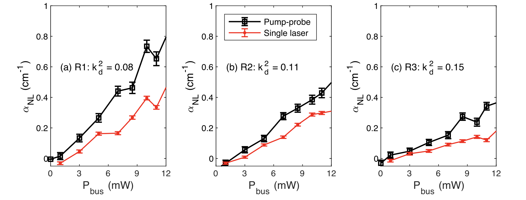
An example of this service was illustrated in a recent publication in which a test and data analysis methodology was developed to extract the nonlinear loss in ring resonators. The measured loss with the proposed continuous-wave pump-probe measurement was 30-40% higher than that obtained by the conventional testing technique of using a single high-power laser.
Mehta et. al, J. Lightwave Technol 42 (9), 3300-3305 (2024)
Mehta et. al, J. Lightwave Technol 42 (9), 3300-3305 (2024)
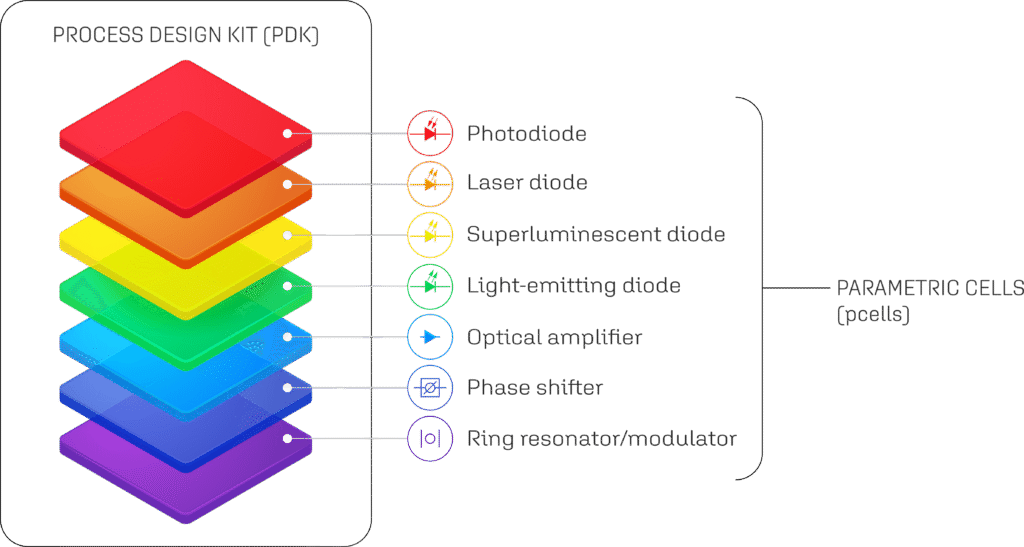
4) Process Design Kit (PDK) and Parametric Cell (pcell) Development
The previous three services were for PIC design houses, while this one is for integrated photonics foundries.
PDKs are a library of all the components which a foundry can make, and PDKs are how foundries communicate with design houses.
Each component in a PDK is expressed as a parametric cell (pcell), which allows the customer to customize components as per their specifications. For example, a laser pcell would allow the designer to modify parameters such as the laser’s grating pitch (wavelength), or length, or current channel width, etc. The pcell would automatically update the parameters of all other laser layers to reflect this high-level parameter change. A pcell allows designers to not have to update tens of other mask layers to reflect a single design change.
Well-designed pcells and PDKs allow designers to design devices and circuits without explicit knowledge of the full fabrication process.